1 - 4
© 2000 IXYS All rights reserved
Symbol
Test Conditions
Maximum Ratings
V
DSS
T
J
= 25
∞
C to 150
∞
C
500
V
V
DGR
T
J
= 25
∞
C to 150
∞
C; R
GS
= 1 M
W
500
V
V
GS
Continuous
±
20
V
V
GSM
Transient
±
30
V
I
D25
T
C
= 25
∞
C
13
A
I
DM
T
C
= 25
∞
C, pulse width limited by T
JM
52
A
I
AR
T
C
= 25
∞
C
13
A
E
AR
T
C
= 25
∞
C
18
mJ
dv/dt
I
S
£
I
DM
, di/dt
£
100 A/
m
s, V
DD
£
V
DSS
,
5
V/ns
T
J
£
150
∞
C, R
G
= 2
W
P
D
T
C
= 25
∞
C
180
W
T
J
-55 ... +150
∞
C
T
JM
150
∞
C
T
stg
-55 ... +150
∞
C
T
L
1.6 mm (0.062 in.) from case for 10 s
300
∞
C
M
d
Mounting torque
1.13/10
Nm/lb.in.
Weight
TO-204 = 18 g, TO-247 = 6 g
Symbol
Test Conditions
Characteristic Values
(T
J
= 25
∞
C, unless otherwise specified)
min.
typ.
max.
V
DSS
V
GS
= 0 V, I
D
= 250
m
A
500
V
V
GS(th)
V
DS
= V
GS
, I
D
= 2.5 mA
2
4
V
I
GSS
V
GS
=
±
20 V
DC
, V
DS
= 0
±
100
nA
I
DSS
V
DS
= 0.8 ∑ V
DSS
T
J
= 25
∞
C
200
m
A
V
GS
= 0 V
T
J
= 125
∞
C
1
mA
R
DS(on)
V
GS
= 10 V, I
D
= 0.5 ∑ I
D25
0.4
W
Pulse test, t
£
300
m
s, duty cycle d
£
2 %
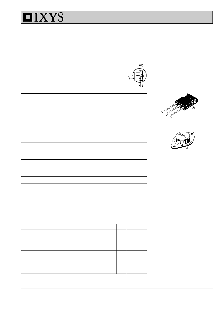
N-Channel Enhancement Mode
High dv/dt, Low t
rr
, HDMOS
TM
Family
TO-247 AD (IXFH)
TO-204 AA (IXFM)
G = Gate,
D = Drain,
S = Source,
TAB = Drain
Features
q
International standard packages
q
Low R
DS (on)
HDMOS
TM
process
q
Rugged polysilicon gate cell structure
q
Unclamped Inductive Switching (UIS)
rated
q
Low package inductance
- easy to drive and to protect
q
Fast intrinsic Rectifier
Applications
q
DC-DC converters
q
Uninterruptible Power Supplies (UPS)
q
Battery chargers
q
Switched-mode and resonant-mode
power supplies
q
DC choppers
q
Temperature and lighting controls
q
Low voltage relays
Advantages
q
Easy to mount with 1 screw (TO-247)
(isolated mounting screw hole)
q
Space savings
q
High power density
D
G
HiPerFET
TM
IXFH
13
N50
V
DSS
= 500 V
Power MOSFETs
IXFM
13
N50
I
D (cont)
= 13 A
R
DS(on)
= 0.4
W
t
rr
£
250 ns
91524D (10/95)
(TAB)
IXYS reserves the right to change limits, test conditions, and dimensions.
2 - 4
© 2000 IXYS All rights reserved
Symbol
Test Conditions
Characteristic Values
(T
J
= 25
∞
C, unless otherwise specified)
min.
typ.
max.
g
fs
V
DS
= 10 V; I
D
= 0.5 I
D25
, pulse test
7.5
9.0
S
C
iss
2800
pF
C
oss
V
GS
= 0 V, V
DS
= 25 V, f = 1 MHz
300
pF
C
rss
70
pF
t
d(on)
18
30
ns
t
r
V
GS
= 10 V, V
DS
= 0.5 ∑ V
DSS
,
27
40
ns
t
d(off)
I
D
= 0.5 ∑ I
D25
, R
G
= 4.7
W
(External)
76
100
ns
t
f
32
60
ns
Q
g(on)
110
120
nC
Q
gs
V
GS
= 10 V, V
DS
= 0.5 ∑ V
DSS
, I
D
= 0.5 ∑ I
D25
15
25
nC
Q
gd
40
50
nC
R
thJC
0.7
K/W
R
thCK
0.25
K/W
Source-Drain Diode
Characteristic Values
(T
J
= 25
∞
C, unless otherwise specified)
Symbol
Test Conditions
min.
typ.
max.
I
S
V
GS
= 0 V
13
A
I
SM
Repetitive; pulse width limited by T
JM
52
A
V
SD
I
F
= I
S
, V
GS
= 0 V,
1.5
V
Pulse test, t
£
300
m
s, duty cycle d
£
2 %
t
rr
T
J
=
25
∞
C
250
ns
T
J
= 125
∞
C
350
ns
Q
RM
T
J
=
25
∞
C
0.6
m
C
T
J
= 125
∞
C
1.25
m
C
I
RM
T
J
=
25
∞
C
9
A
T
J
= 125
∞
C
15
A
I
F
= I
S
-di/dt = 100 A/
m
s,
V
R
= 100 V
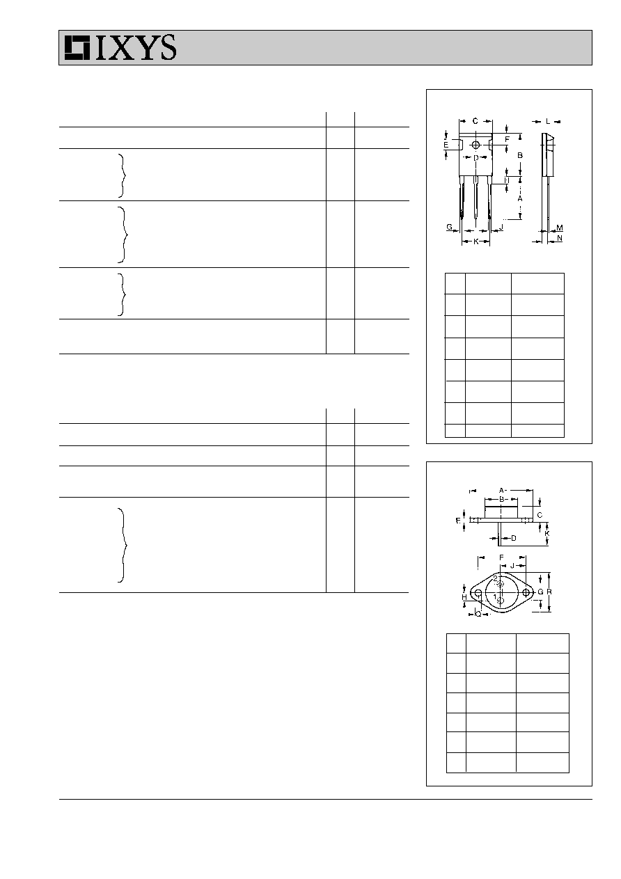
TO-247 AD (IXFH) Outline
Dim. Millimeter
Inches
Min.
Max.
Min.
Max.
A
19.81 20.32
0.780 0.800
B
20.80 21.46
0.819 0.845
C
15.75 16.26
0.610 0.640
D
3.55
3.65
0.140 0.144
E
4.32
5.49
0.170 0.216
F
5.4
6.2
0.212 0.244
G
1.65
2.13
0.065 0.084
H
-
4.5
-
0.177
J
1.0
1.4
0.040 0.055
K
10.8
11.0
0.426 0.433
L
4.7
5.3
0.185 0.209
M
0.4
0.8
0.016 0.031
N
1.5
2.49
0.087 0.102
TO-204 AA (IXFM) Outline
Dim.
Millimeter
Inches
Min.
Max.
Min.
Max.
A
38.61 39.12
1.520 1.540
B
19.43 19.94
- 0.785
C
6.40
9.14
0.252 0.360
D
0.97
1.09
0.038 0.043
E
1.53
2.92
0.060 0.115
F
30.15
BSC
1.187
BSC
G
10.67 11.17
0.420 0.440
H
5.21
5.71
0.205 0.225
J
16.64 17.14
0.655 0.675
K
11.18 12.19
0.440 0.480
Q
3.84
4.19
0.151 0.165
R
25.16 25.90
0.991 1.020
IXFH 13N50
IXFH 13N50
IXYS MOSFETS and IGBTs are covered by one or more of the following U.S. patents:
4,835,592
4,881,106
5,017,508
5,049,961
5,187,117
5,486,715
4,850,072
4,931,844
5,034,796
5,063,307
5,237,481
5,381,025
3 - 4
© 2000 IXYS All rights reserved
IXFH 13N50
IXFH 13N50
T
J
- Degrees C
-50
-25
0
25
50
75
100
125
150
BV
/
V
G(
th
)
- N
o
rm
a
lize
d
0.5
0.6
0.7
0.8
0.9
1.0
1.1
1.2
BV
DSS
T
C
- Degrees C
-50
-25
0
25
50
75
100
125
150
I
D
-
A
m
p
e
r
e
s
0.0
2.5
5.0
7.5
10.0
12.5
15.0
T
J
- Degrees C
-50
-25
0
25
50
75
100
125
150
R
DS
(
on)
- N
o
r
m
a
liz
e
d
0.50
0.75
1.00
1.25
1.50
1.75
2.00
2.25
2.50
I
D
- Amperes
0
5
10
15
20
25
R
DS
(
on)
- N
o
r
m
a
liz
e
d
0.8
0.9
1.0
1.1
1.2
1.3
1.4
V
GS
= 10V
T
J
= 25∞C
V
GS
- Volts
0
1
2
3
4
5
6
7
8
9
10
I
D
- A
m
p
e
re
s
0
5
10
15
20
25
T
J
= 25∞C
V
DS
- Volts
0
5
10
15
20
I
D
- A
m
p
e
re
s
0
5
10
15
20
25
6V
5V
7V
8V
V
GS(th)
13N50
I
D
= 6A
V
GS
= 15V
V
GS
=10V
T
J
= 25∞C
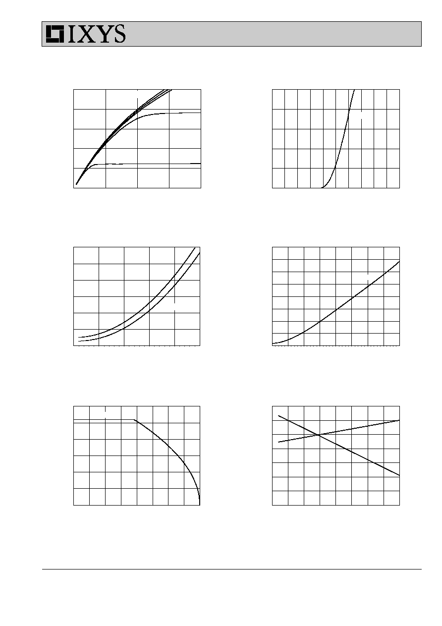
Fig. 1 Output Characteristics
Fig. 2 Input Admittance
Fig. 5 Drain Current vs.
Fig. 6 Temperature Dependence of
Case Temperature
Breakdown and Threshold Voltage
Fig. 3 R
DS(on)
vs. Drain Current
Fig. 4 Temperature Dependence
of Drain to Source Resistance
4 - 4
© 2000 IXYS All rights reserved
IXFH 13N50
IXFH 13N50
V
SD
- Volt
0.00
0.25
0.50
0.75
1.00
1.25
1.50
I
S
- Am
per
es
0
5
10
15
20
25
Time - Seconds
0.00001
0.0001
0.001
0.01
0.1
1
10
Th
ermal
Res
ponse
-
K/
W
0.01
0.10
1.00
D = 0.2
D=0.02
D = 0.5
D = 0.1
D = 0.05
D=0.01
Single Pulse
V
DS
- Volts
0
5
10
15
20
25
Cap
a
ci
tanc
e -
pF
0
500
1000
1500
2000
2500
3000
3500
4000
C
rss
C
oss
C
iss
Gate Charge - nCoulombs
0
25
50
75
100
V
GS
- V
o
lts
0
1
2
3
4
5
6
7
8
9
10
I
D
= 6.5A
V
DS
= 250V
V
DS
- Volts
1
10
100
I
D
-
Amperes
0.1
1
10
100
10µs
100µs
1ms
10ms
100ms
Limited by R
DS(on)
I
G
= 10mA
T
J
= 125∞C
T
J
= 25∞C
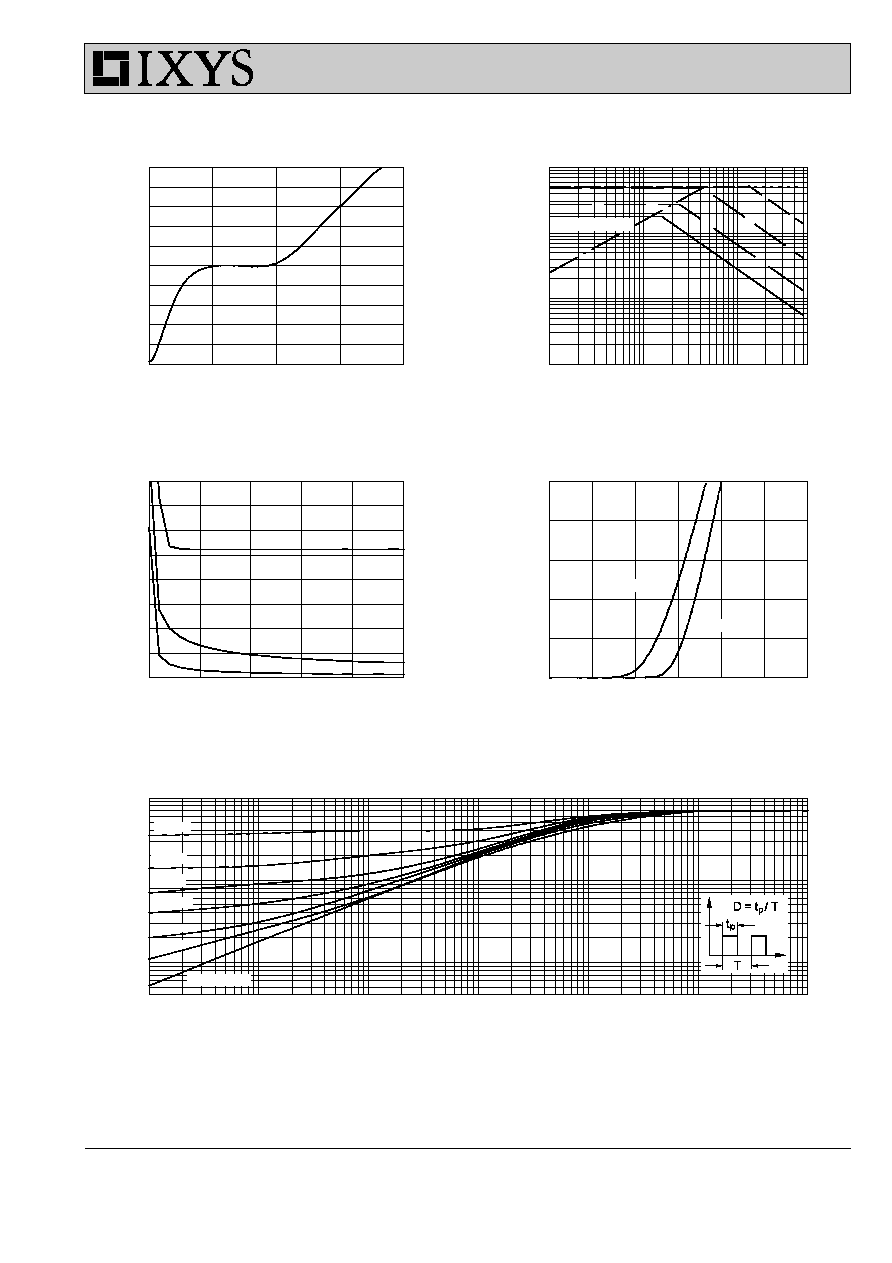
Fig.7 Gate Charge Characteristic Curve
Fig.8 Forward Bias Safe Operating Area
Fig.9 Capacitance Curves
Fig.10 Source Current vs. Source
to Drain Voltage
Fig.11 Transient Thermal Impedance